In high energy accelerators, where particles are travelling in the relativistic regime, beam bending and focusing is usually achieved by magnets. However, at kinetic energies below 100 keV, magnets become less effective for beam control. This is where electrostatic fields offer a number of distinct advantages.
Low energy antimatter and ion beam facilities rely on electrostatic beam transfer lines, as well as electrostatic elements existing in storage rings. To date, there was no analogon to the commonly used Hall probe that could precisely map the field created by electrostatic ion optics. Therefore, one had to rely on simulations like the one exemplified below to study the effects from grounded shields, manufacturing tolerances or misplacements.
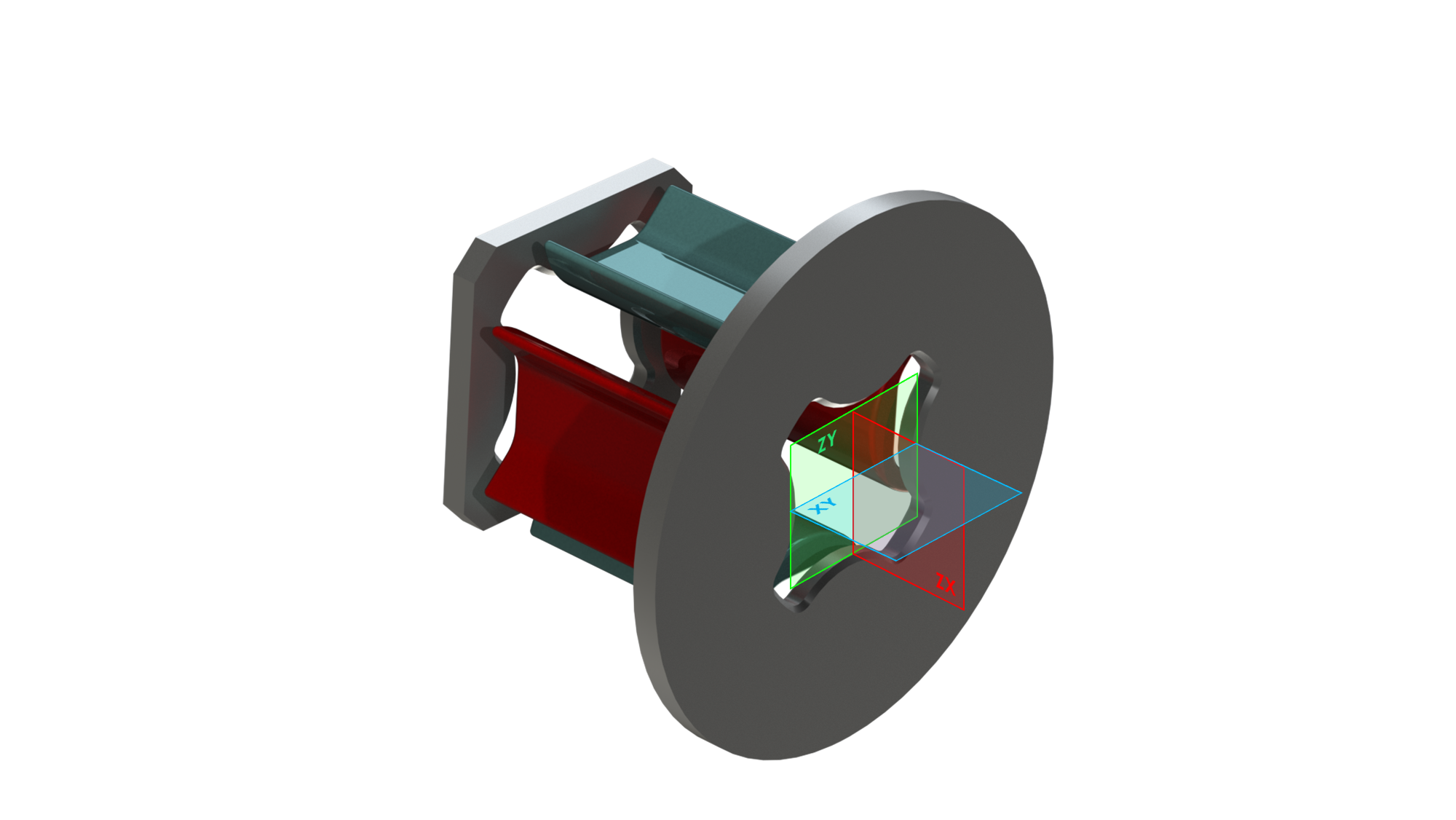
Electrostatic quadrupole with grounded shield in in simulation.
(Image copyright: Physical Review Letters and Volodymyr Rodin, University of Liverpool)
A paper by A. Kainz et al. that was recently published in Physical Review Letters, describes a new method to precisely map the electrostatic field in an arbitrary 3D volume, with a microsensor. In a collaboration between researchers from Vienna, CERN and the University of Liverpool/Cockcroft Institute, the sensor was extensively tested to characterize an electrostatic quadrupole magnet from one of the ELENA beam transfer lines.
The functioning principle of the sensor is based on the electrostatic induction occurring inside a conducting body. The charged surfaces of the polarized conductor are, due to the external field E, subject to an electrostatic force Fe = Q E. This force is used to deflect a spring-suspended proof mass of a microelectromechanical sensor (MEMS). The deflection is recorded in an optical way, and compared to a reference system etched on the chip.
For the purpose of probing the quadrupole field, the MEMS chip was fixed inside a 3D-printed dielectric holder and connected via optical fibres to the readout electronics, placed at a remote location from the assembly. Except for the silicon part of the MEMS chip, only dielectric materials are used in the probe to minimize the sensor’s influence. The light is guided through the chip and reflected by a small right-angle prism and fed back to the fibre.
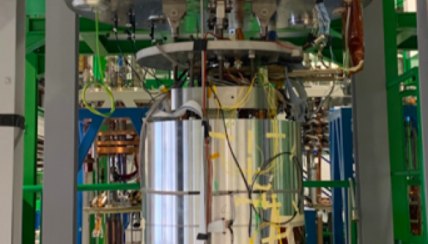
A photograph of the experimental setup us shown below:
Sensor test stand using ELENA quadrupole. ELENA is a compact ring for cooling and further deceleration of 5.3 MeV antiprotons delivered by the CERN Antiproton Decelerator. The ultimate physics goal is to perform spectroscopy on antihydrogen atoms at rest and to investigate the effect of the gravitational force on matter and antimatter. (Image: Wilfried Hortshitz, Danube University Krems)
Experimental results have shown that a remarkable spatial resolution can be achieved for fields with sufficiently low curvature. Measurements have also confirmed that electrostatic elements behave largely like numerical simulations predict.
Future accelerator projects, such as a storage ring to measure the electric dipole moment, will depend on the use of electrostatic elements. A field homogeneity of 1⋅10-4 or better will be required, which corresponds to extreme mechanical fabrication tolerances of only a few micrometres. A precise field measurement technique as this 3D mapping of electrostatic fields offers an interesting opportunity to relax these requirements. It offers a powerful method to mitigate any effects from tolerances, by sorting electrostatic elements or even the active compensation of unwanted effects.
The collaboration now plans to research and develop a combined sensor that can measure all three field axes at once, as well as strategies to completely eliminated effects from spatial offset.
Further reading:
- A. Kainz et al., Distortion-free measurement of electric field strength with a MEMS sensor, Nature Electronics 1 (2018).
- A. Kainz et al., Noninvasive 3D field mapping of complex static electric fields, Phys. Rev. Lett. 122, 244801 (2019).

.png)


